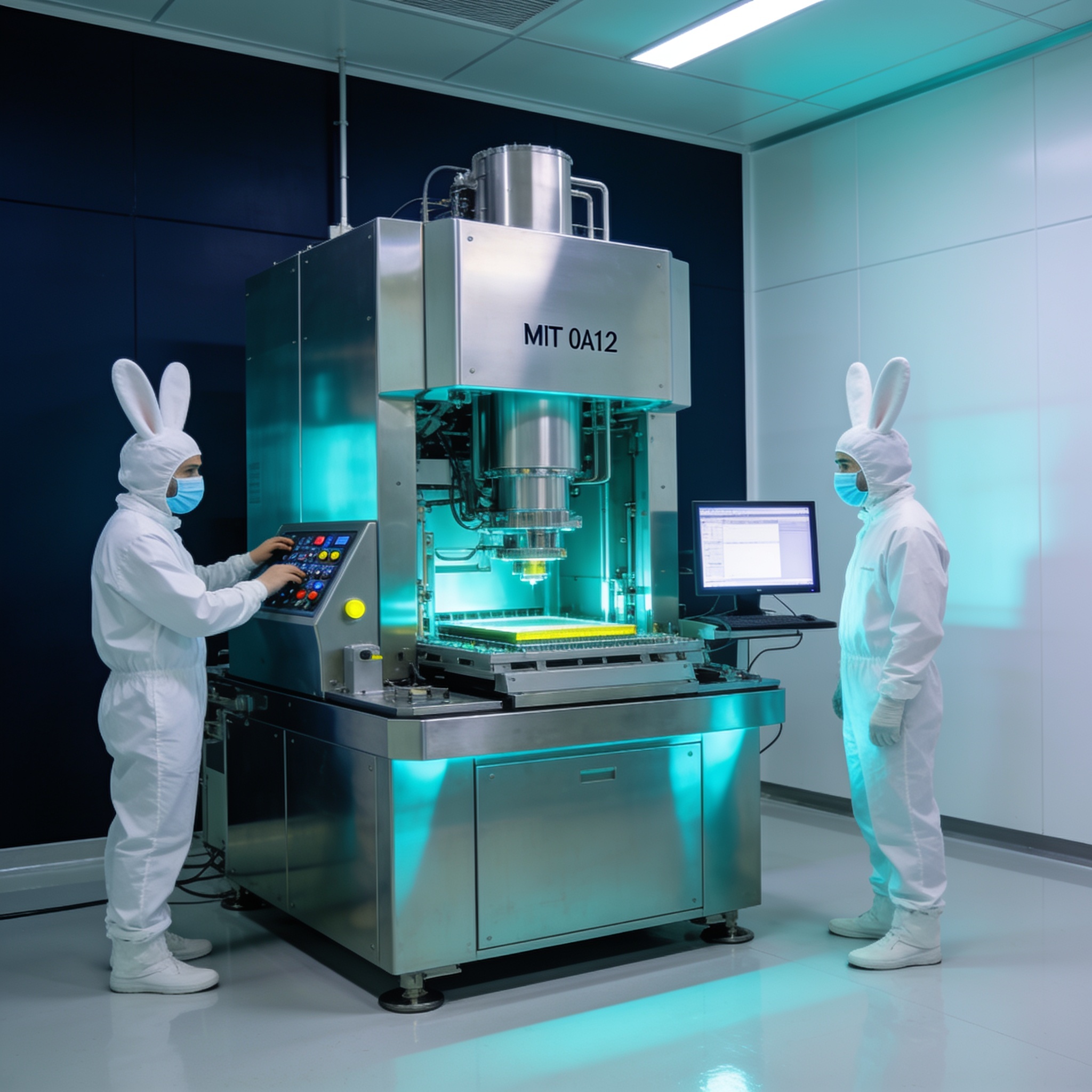
On September 16, 2026, Spain’s National Research Council (CSIC) inaugurated a Quantum Nanofabrication Area at the Institute of Microelectronics of Barcelona (IMB-CNM). The €6 million investment, funded by Spain’s PERTE Chip program and the European Union’s NextGenerationEU recovery fund, equips the facility with advanced lithography and microscopy systems for prototyping quantum hardware components, including quantum processing units (QPUs) and quantum key distribution (QKD) devices.
What They’re Actually Building
The new cleanroom is not a quantum computer. It is a shared fabrication line designed to produce the physical chips that underpin quantum technologies. The toolset includes electron-beam lithography for patterning sub-micron features, along with atomic force and scanning electron microscopes for inspection. These are standard instruments for research-scale device fabrication, but their availability in a dedicated quantum prototyping environment removes a bottleneck for Spanish research groups.
The facility operates under the QuARC-CSIC initiative, which consolidates 36 research groups across Spain working on quantum computing, communication, sensing, and simulation. By providing in-house nanofabrication, CSIC aims to accelerate the cycle from design to testable device—a critical step for superconducting qubits, spin qubits in silicon, and photonic quantum chips. The investment is modest by global standards: a single extreme ultraviolet (EUV) lithography tool for high-volume semiconductor manufacturing costs over €150 million. This is a prototyping line, not a production fab.
Spain’s quantum hardware ambitions span multiple qubit platforms. The IMB-CNM itself has expertise in superconducting circuits and silicon-based devices. The new area will allow researchers to iterate on Josephson junctions, quantum dots, and integrated photonic circuits without waiting for external foundry runs. For QKD, the facility can fabricate single-photon sources and detectors, essential for secure communication networks. The cleanroom’s capabilities are tailored for low-volume, high-mix prototyping—exactly what academic and early-stage startup teams need.
Winners and Losers
The immediate beneficiaries are the 36 QuARC-CSIC groups and any Spanish quantum startups that gain access. Previously, these teams had to book time at foreign cleanrooms—such as those at imec in Belgium or Leti in France—adding cost, delay, and logistical friction. Domestic prototyping capability could shorten iteration cycles and keep intellectual property closer to home. Spanish quantum startups like Qilimanjaro Quantum Tech (superconducting qubits) and LuxQuanta (continuous-variable QKD) stand to gain from local prototyping, potentially reducing their time-to-demonstration.
No established quantum hardware company is directly threatened. The facility does not compete with IBM’s in-house fabrication in New York, Google’s Santa Barbara lab, or the large foundries that serve the semiconductor industry. Instead, it fills a gap in the European quantum supply chain. If the facility succeeds, it could strengthen Spain’s position in EU-funded quantum projects and attract talent that might otherwise go to Germany, France, or the Netherlands.
For the broader quantum ecosystem, more accessible nanofabrication lowers the barrier for experimental physicists and engineers to test novel qubit designs. That could accelerate the pace of innovation in error mitigation and materials science, areas where rapid prototyping is essential. However, the facility’s impact will depend on whether it can maintain high uptime, process reliability, and open access policies—challenges that have plagued similar academic cleanrooms.
The Bigger Picture
In 2026, quantum computing remains in the noisy intermediate-scale quantum (NISQ) era, with error correction still years away from practical deployment. Governments worldwide are investing in quantum infrastructure to secure future capabilities. The EU’s Quantum Flagship has allocated €1 billion over ten years, and the European Chips Act aims to double the bloc’s semiconductor market share. Spain’s PERTE Chip program, which funded this facility, is part of that push.
Comparable national efforts include Germany’s Fraunhofer quantum computing initiative, which provides cloud access to IBM quantum systems, and France’s Maison du Quantique, a coordination hub. The Barcelona nanofabrication area is more hands-on: it gives researchers the tools to build devices, not just use them. That aligns with the EU’s goal of reducing dependence on non-European suppliers for critical quantum components.
The facility also complements existing European infrastructure. For example, imec’s 300-mm cleanroom in Leuven focuses on CMOS-compatible quantum dot qubits, while Leti in Grenoble has a strong photonics program. Barcelona’s niche could be rapid prototyping of hybrid superconducting-photonic circuits or specialized QKD chips. The €6 million investment is a fraction of the €2.4 billion that Germany has pledged for quantum technologies, but it targets a specific fabrication gap that larger hubs may not address with the same flexibility.
The Signal
The signal here is that Spain is moving beyond quantum theory and software into the physical fabrication of quantum devices. The €6 million price tag is small relative to the billions poured into quantum computing globally, but it addresses a specific, practical need: a domestic cleanroom for prototyping. The real test will be whether the facility produces working quantum chips that demonstrate measurable coherence or entanglement metrics. The milestone to watch is the first functioning qubit or QKD transmitter fabricated entirely within this cleanroom and validated by an independent group.
What this reveals is a strategic bet: that quantum hardware sovereignty requires not just algorithms and cloud access, but the ability to build and test physical devices at home. If the facility yields competitive qubit performance, it could attract industrial partners and additional EU funding. If not, it risks becoming another underutilized academic cleanroom. For now, the Barcelona cleanroom is a necessary, if incremental, step toward a European quantum supply chain.
“Spain’s new €6M quantum nanofabrication area gives its 36 research groups a domestic prototyping line for QPUs and QKD components, reducing reliance on foreign cleanrooms.”