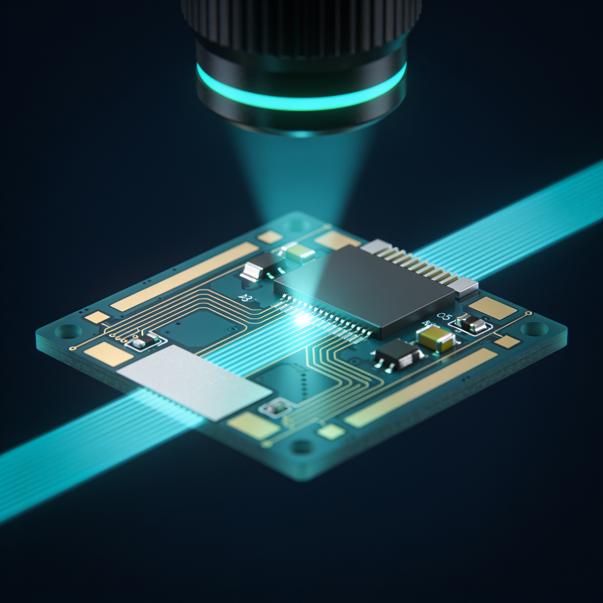
The Problem Nobody Solved
Photonic quantum computers have spent the past five years proving they can outperform classical machines on carefully chosen sampling tasks. The problem is that the most famous demonstrations remain fragile optical experiments: tabletop Gaussian boson sampling setups require stringent optical alignment, suffer from phase instability, and offer limited programmability once built. The authors behind the new preprint — whose institutional affiliation is not listed in the supplied arXiv metadata — investigate whether a single chip can remove those barriers without sacrificing the photon numbers that make quantum advantage credible. [arXiv:2609.11922]
That question matters because quantum advantage claims in photonics have been hard to scale. Free-space mirrors and fiber loops can deliver large interference networks, but they are difficult to stabilize across thousands of optical paths. A chip-scale architecture would bring fabrication discipline, but it demands simultaneous low loss, high precision, and high-speed modulation across many integrated components. Until now, no one had reported a monolithic Gaussian boson sampling processor beyond 10,000 detected photons.
The core obstacle is not simply putting more light on a chip. It is preserving quantum coherence across temporal and spatial modes while actively controlling the interferometer at gigahertz rates. In an integrated platform, every waveguide bend, splitter, and delay line adds loss; every modulator adds phase noise. Solving that combination in one thin-film lithium niobate chip is what makes the demonstration unusual.
The Core Finding
The team reports the first chip-scale space-time multiplexed Gaussian boson sampling system. It operates at a 4-GHz clock rate and records detection events of up to 11,059 photons within 1 millisecond. The hardware integrates high-speed electro-optic modulators, on-chip delay lines, and a time-space multiplexed interferometric network on a thin-film lithium niobate chip. In the abstract, the authors describe the platform as:
monolithically integrating high-speed electrooptic modulators, on-chip delay lines, and a time-space multiplexed interferometric network on a thin-film lithium niobate chip
Think of it like replacing a room-sized optical table with an integrated circuit that steers, delays, and interferes photons at gigahertz speed. In Gaussian boson sampling, squeezed light enters a network of many optical paths, and the output photon pattern is sampled. The chip-scale version compresses those paths into time and space bins, allowing many modes to share physical hardware without losing the interference pattern.
Beyond benchmarking quantum advantage, the same photonic hardware is reconfigured into a GBS-powered world model for modelling physical dynamics. That configuration achieves lower prediction error with fewer trainable readout parameters than a classical echo state network baseline. This second result suggests that the processor may have a use beyond sampling benchmarks, as a photonic recurrent reservoir for time-series modelling.
The State of the Field
Previous photonic quantum advantage experiments built the case for Gaussian boson sampling as a leading platform. Jiuzhang, reported by Zhong et al. in 2020, and Borealis, reported by Madsen et al. in 2022, demonstrated large-scale sampling but relied on tabletop or fiber-based interferometers. Those systems faced the same practical barriers named in the new abstract: stringent optical alignment, phase instability, and limited programmability.
What changed is the substrate. Thin-film lithium niobate allows strong electro-optic modulation and tight optical confinement, making it possible to combine fast control and low-loss routing on one chip. The new work does not simply miniaturize a GBS experiment; it uses time-space multiplexing to make a compact system operate at a 4-GHz clock rate. This approach is distinct from earlier silicon photonic GBS attempts because lithium niobate offers both fast modulation and relatively low propagation loss in the telecom band.
The broader quantum computing landscape in late 2026 includes superconducting, trapped-ion, neutral-atom, and photonic platforms. Photonic approaches attract attention for room-temperature operation and potential semiconductor-style manufacturing, but they have historically struggled with integration and loss. The new result sits inside an active effort to make photonic quantum hardware manufacturable, led by academic groups and companies working on integrated photonics.
From Lab to Reality
For scientists, this result provides a reconfigurable chip-scale testbed for studying quantum advantage and quantum simulation without rebuilding optical paths between experiments. It also opens a path toward benchmarking GBS as a physical dynamics model rather than only as a computational sampling task. The world model result, with fewer trainable readout parameters than a classical echo state network, suggests that photonic processors could efficiently encode temporal information for machine learning and for modelling complex physical systems.
For engineers, the monolithic integration of modulators, delay lines, and interferometric networks on thin-film lithium niobate is a concrete blueprint for chip-scale photonic processors. That could influence design of high-speed optical interconnects, integrated sensors, and specialized quantum computing modules. Because the system runs at 4 GHz, it also stresses electronics and detector interfaces in a way that may accelerate development of fast cryogenic and room-temperature photodetectors.
Although the paper does not address quantum cryptography directly, a chip-scale interferometric platform with fast phase control could eventually inform quantum communication hardware. For investors, the work affects the emerging photonic quantum hardware segment. Some market analyses place the broader quantum computing market above $6.5 billion by 2030, with integrated photonics expected to claim a growing share as manufacturable platforms mature.
What Still Needs to Happen
The first remaining challenge is loss. Scaling beyond 10,000 detected photons will require wafer-scale fabrication that maintains low waveguide loss and high-precision modulators simultaneously. Thin-film lithium niobate waveguides have improved rapidly, but manufacturing variability remains high compared with established silicon photonics. Each additional spatial or temporal mode multiplies the chance of a photon being lost before detection.
The second challenge is detection and control overhead. Operating at 4 GHz demands fast single-photon detectors and phase-stable electronics that can keep up with on-chip routing. Many current detector arrays cannot sustain high count rates across all modes without saturation or added jitter. Groups such as PsiQuantum and Xanadu continue to develop integrated photonic architectures for scalable quantum hardware, while academic thin-film lithium niobate research programs focus on reducing propagation loss and increasing modulator bandwidth.
There is no immediate path to fault-tolerant quantum computing here. The reported system is not a universal quantum computer and does not perform quantum error correction. Even with these results, a useful fault-tolerant photonic quantum computer remains roughly a decade away. The realistic next step is to improve chip yield, detector efficiency, and reconfigurability so that chip-scale GBS can be tested against the best classical algorithms rather than only against an ESN baseline.
Conclusion
In short: quantum advantage now has a chip-scale photonic implementation reporting 11,059 photon detection events within 1 millisecond, moving Gaussian boson sampling from fragile free-space optics to monolithic thin-film lithium niobate hardware. The remaining barriers are real, but the integrated platform gives researchers a new tool to attack them.