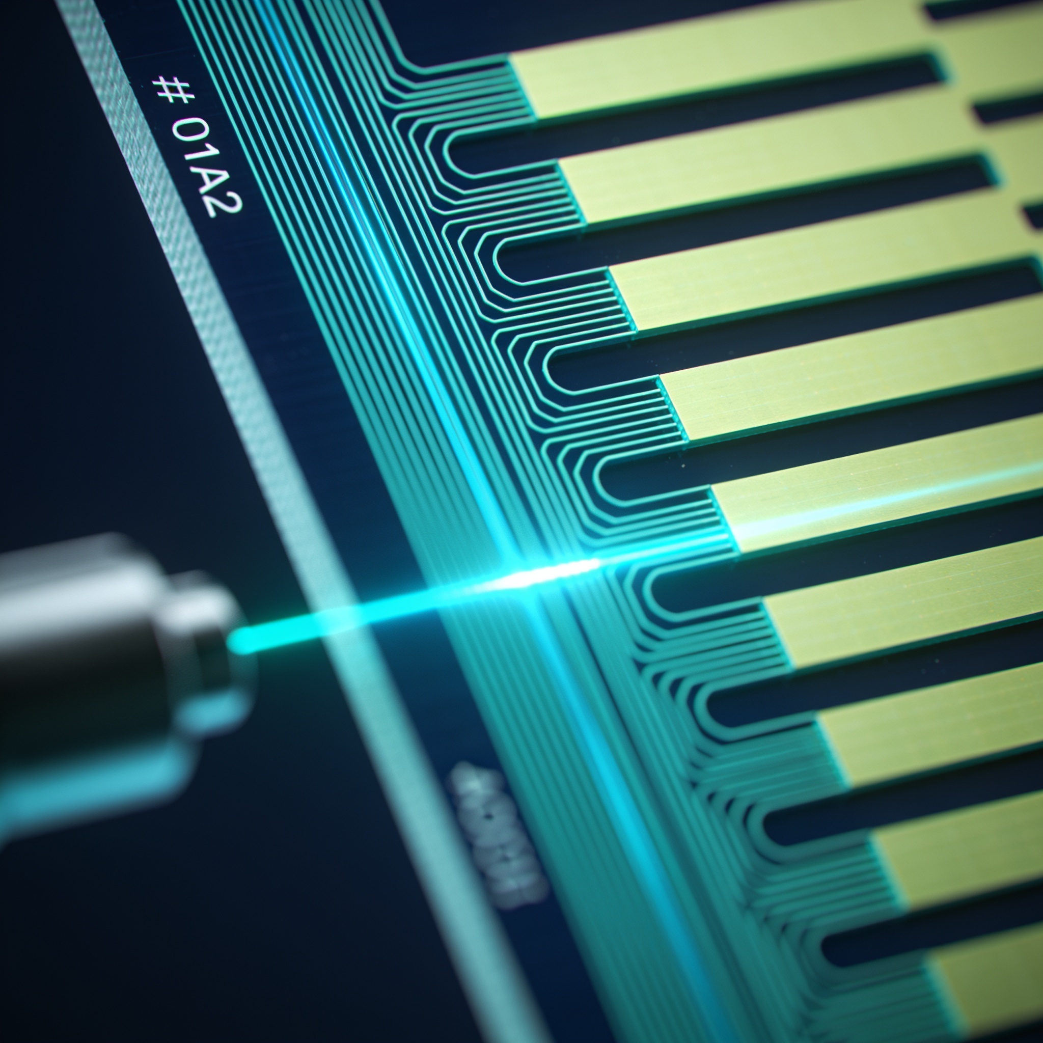
For years, Gaussian boson sampling experiments have demonstrated quantum advantage using table-sized optical setups painstakingly aligned by hand. Those systems are fragile, scarcely programmable, and utterly unscalable. Now researchers have achieved a milestone that could change the narrative: a chip-scale system that operates at 4 billion cycles per second and registers more than 11,000 photons in a fraction of a second. [arXiv:2609.11922]
The Core Finding
The team forged the first chip-scale space-time multiplexed Gaussian boson sampling processor by monolithically integrating high-speed electro-optic modulators, on-chip delay lines, and a time-space multiplexed interferometric network onto a single thin-film lithium niobate chip. The hardware runs at a 4-GHz clock rate, generating detection events of up to 11,059 photons within one millisecond—an order-of-magnitude leap in simultaneous photon throughput for an integrated photonic circuit. Think of the chip as a high-speed photon racetrack where pulses of squeezed light zip through precisely timed routes, interfering at each turn, while modulators switch paths every quarter-nanosecond. This compact engine not only outperforms earlier table-top counterparts but also reconfigures into a GBS-powered world model that predicts physical dynamics with lower error and fewer trainable readout parameters than a classical echo state network.
"We report the first chip-scale space-time multiplexed Gaussian boson sampling system … operating at a 4-GHz clockrate with detection events of up to 11,059 photons within 1 millisecond."
The State of the Field
Before this work, flagship Gaussian boson sampling demonstrations such as Jiuzhang (2020) and Borealis (2022) relied on networks of free-space optics, fiber loops, and painstaking phase calibration. Those machines proved quantum advantage but shared a fatal weakness for practical deployment: their size and alignment sensitivity made them near-impossible to scale or reconfigure. The new chip-side approach breaks that paradigm by adopting thin-film lithium niobate, a material prized for its strong electro-optic coefficient and ultralow optical loss. Recent advances in wafer-scale fabrication of this platform have finally allowed researchers to combine modulators, delay lines, and a full interferometric mesh on a millimeter-scale die. The result is a programmable, alignment-free system that marries the raw speed of photonics with the integration density needed for field-deployable quantum hardware.
From Lab to Reality
For scientists, the chip provides a tuneable sandbox for exploring quantum advantage beyond sampling—the team’s world model shows it can already act as a reservoir computer with inherent quantum knots that classical networks struggle to mimic. Engineers gain a blueprint for building compact, high-speed photonic coprocessors that could slot into data centers for optimization, machine learning, and real-time simulation. The demonstration that the same photonic fabric can be reprogrammed for both boson sampling and physical dynamics modeling hints at a versatile acceleration layer. Investors eyeing the photonic quantum computing market, which analysts project will reach several billion dollars by the mid-2030s, now have a concrete signal that chip-scale integration is crossing from academic curiosity to engineered prototype. While full fault-tolerant quantum computing remains distant, application-specific processors for sampling and simulation could arrive within a decade.
What Still Needs to Happen
Despite its record photon count, the platform still relies on off-chip pump lasers and photon-number-resolving detectors that have yet to be integrated. Loss inside the on-chip delay lines and modulators eats into fidelity, and extending the circuit to larger sizes demands a further reduction in propagation loss—work that groups at PsiQuantum and Xanadu are tackling with alternative material stacks. The processor also lacks native sources of squeezed light on chip, a milestone that would close the loop on a fully monolithic system. Boson sampling itself lacks a known error-correction threshold, so whatever advantage it offers does not directly translate to fault-tolerant quantum computing. The team’s world model demonstration is encouraging, yet the range of physical problems that a GBS-powered reservoir can solve remains to be mapped. All told, this is a proof-of-principle that massive photon multiplexing is feasible on a chip, but achieving industrial-grade reliability and scale will likely require another five to ten years of intensive engineering.
In short: a chip-scale space-time multiplexed Gaussian boson sampling processor has shattered the 10,000-photon barrier, offering a clear path to scalable photonic quantum advantage and real-world physical simulation.