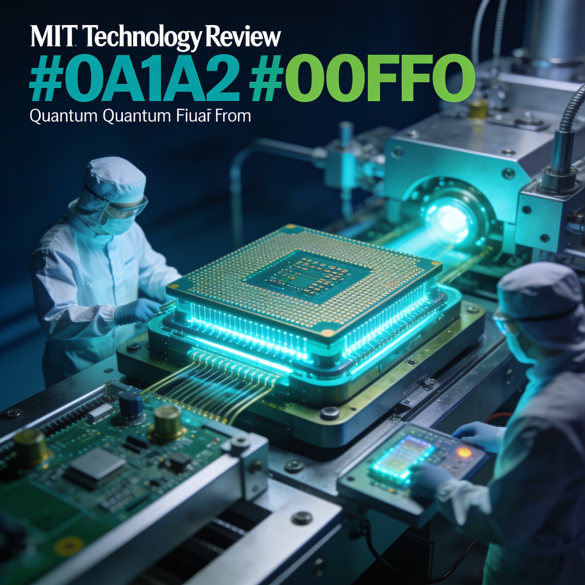
In a September 2026 interview with The Quantum Insider, Brian Gaucher, an IBM veteran and co-chair of the Engineering Research Visioning Alliance (ERVA) report on quantum technologies, delivered a blunt assessment: the quantum computing field has solved enough physics. The obstacle now is engineering—specifically, the “lab to fab” transition that turns fragile qubit demonstrations into manufacturable, reliable systems. Gaucher’s warning comes as the U.S. quantum science base remains strong, but global competitors are accelerating their engineering capabilities.
What the ERVA Report Actually Says
The ERVA report, Engineering Research to Advance Quantum Technologies, identifies a set of engineering gaps that no amount of physics research will close. These include scalable qubit fabrication processes, cryogenic control electronics, high-density interconnects, thermal management for dilution refrigerators, and packaging that preserves coherence while enabling mass production. The report frames these as system-level problems, not component-level tweaks. “We’re not waiting for a new physics breakthrough. We’re waiting for manufacturing yields, testability, and repeatability,” Gaucher said, summarizing the report’s central thesis.
This shift mirrors the semiconductor industry’s own history: the transistor was a physics triumph in 1947, but the integrated circuit became an engineering triumph in the 1960s. Quantum computing, Gaucher argues, is at a similar inflection point. IBM’s own roadmap, targeting 100,000 qubits by 2033, explicitly demands engineering advances in chip packaging, cryo-CMOS control, and automated calibration. Without those, the roadmap remains aspirational. The ERVA report pushes for a national engineering research initiative focused on quantum manufacturing, akin to the DARPA programs that enabled VLSI scaling.
Winners and Losers
The companies best positioned to benefit from an engineering-first focus are those with deep semiconductor manufacturing expertise. IBM, with its in-house fabrication and packaging heritage, and Intel, which is already leveraging its transistor fabs for silicon spin qubits, have intrinsic advantages. Similarly, TSMC’s growing involvement in cryogenic CMOS for quantum control chips signals that the foundry model could extend to quantum. Smaller pure-play quantum startups—especially those relying on bespoke laboratory setups—face a harder road. IonQ’s trapped-ion systems, while less dependent on lithographic scaling, still require integrated photonics and vacuum packaging that demand manufacturing rigor. Quantinuum’s approach with trapped ions in surface traps faces similar engineering burdens.
Losers are research organizations that treat quantum exclusively as a physics problem. National labs and universities, while still vital for fundamental insights, must pivot resources toward engineering design and test infrastructure. Gaucher noted that China’s quantum program is investing heavily in engineering talent and fabrication facilities, aiming to close the gap not through new algorithms but through scalable production. If the U.S. does not prioritize quantum engineering, the lab-to-fab gap could become a strategic vulnerability.
The Bigger Picture
Gaucher’s comments arrive as the quantum industry in 2026 wrestles with the NISQ era’s endgame. Error correction demonstrations have crossed the break-even point, but logical qubit counts remain in the single digits. Scaling to 100 or 1,000 logical qubits requires thousands of physical qubits, each with consistent performance. The ERVA report’s engineering focus aligns with the U.S. CHIPS Act’s manufacturing incentives, though quantum has yet to receive dedicated fab-scale funding. The EU’s Quantum Flagship and Japan’s Moonshot program have both identified quantum engineering as a priority, setting up a global race for fabrication and packaging talent.
Comparable milestones in other fields show the pattern: superconducting qubits have improved coherence times tenfold since 2015, but the variation from wafer to wafer remains a yield problem. The industry’s shift toward engineering is not a downgrade—it’s a sign of maturity. When the hardest problems are statistical process control and interconnect density, the technology is on the cusp of leaving the lab.
The Signal
The signal here is not that quantum computing has stalled; it’s that the conversation has moved from “can we build a qubit?” to “can we build a million identical ones?” Gaucher’s framing reveals that the next phase of quantum development will be won or lost on factory floors, not in physics journals. The specific technical milestone that would validate this claim is a repeatable, multi-wafer run of superconducting qubits with coherence times and gate fidelities within a tight distribution—comparable to the semiconductor industry’s Cpk metrics. No company has publicly demonstrated that yet, but the ERVA report makes clear that this is the real target.
“The lab-to-fab gap is the real limiter for quantum computing; without solving manufacturing, we remain stuck in the NISQ era indefinitely.”
In short: the quantum engineering bottleneck is now the primary constraint on progress, and the race to build a quantum fab is the race to win the quantum era.