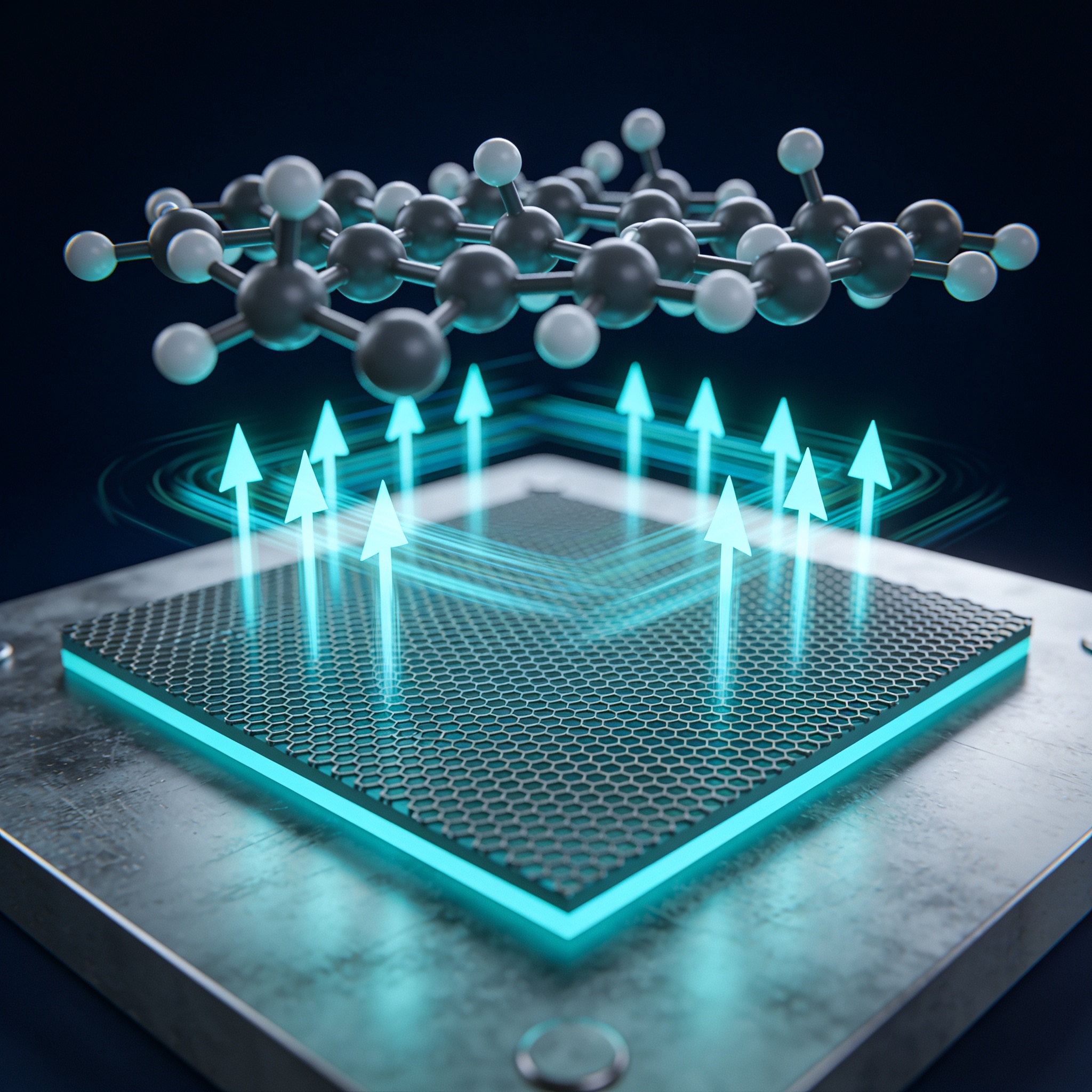
For decades, researchers have sought to control how energy moves through molecular assemblies by manipulating the electromagnetic environment around them. The challenge has always been that once a molecular aggregate is fabricated—whether it aligns dipoles head-to-tail in a J-type configuration or side-by-side in an H-type arrangement—that coupling pattern is essentially fixed. You cannot flip a switch and turn one into the other mid-experiment. A research team has now shown that a single-atom-thick layer of graphene, placed on a metallic substrate, can do exactly that: dynamically invert the coupling type by simply changing the graphene's surface conductivity. [arXiv:2609.02933]
The Core Finding
The paper demonstrates that when molecular aggregates are positioned near a graphene monolayer backed by a metal substrate, varying the graphene's surface conductivity—achievable through electrostatic gating—shifts the parameter space where dipole-dipole coupling inversion occurs. The researchers model nearly H-type and nearly J-type aggregates and find that the transition between coupling regimes becomes tunable. As the abstract states, "as the surface conductivity of the graphene is varied, there is a corresponding change in the parameter region over which coupling inversion is predicted." Think of it like a dimmer switch for molecular interactions: instead of replacing the entire lighting fixture to change the room's character, you simply adjust the dial. The graphene layer acts as that dial, continuously modifying the photonic environment that mediates how molecules talk to each other. The key metric is not a simple error-rate reduction but a qualitative shift: the system moves from predicting inversion only in narrow, hard-to-access conditions to making that inversion accessible within a single experimental run by sweeping the gate voltage.
The State of the Field
Environmental modification of dipole-dipole interactions has a long history in molecular photophysics. Prior work established that placing molecular aggregates near metallic surfaces, plasmonic nanostructures, or optical cavities can alter coupling strengths and even flip the sign of the interaction under specific geometric conditions. What has been missing is dynamical control. Previous proposals required fabricating different structures for each coupling regime or operating at fixed, predetermined distances. This paper introduces a fundamentally different approach: using graphene's electrically tunable conductivity to modulate the environment in real time. The broader quantum computing landscape is currently wrestling with a parallel challenge—how to make qubit interactions switchable without introducing noise. While this paper focuses on molecular excitonic systems rather than qubit platforms directly, the conceptual bridge is clear: tunable dipole-dipole coupling is a building block for controlled energy transfer, which underpins proposals for excitonic quantum information processing and light-harvesting optimization.
From Lab to Reality
For scientists studying quantum energy transport, this work unlocks an experimental knob that did not previously exist. Rather than synthesizing a new sample for every data point in a coupling-strength sweep, researchers can now envision a single device where the gate voltage on the graphene layer scans through the entire parameter space. This dramatically accelerates the search for coupling-inversion signatures that have been theoretically predicted but experimentally elusive. For engineers working on molecular-scale optoelectronics, the finding suggests a route toward switchable light-emitting or light-harvesting devices where the collective optical response can be toggled between H-type (blue-shifted, weak emission) and J-type (red-shifted, superradiant) behavior on demand. The quantum error correction market, estimated at $1.2 billion by 2030 according to industry projections, may seem distant from molecular aggregates, but the underlying physics—controlling dipole-mediated interactions through tunable environments—is directly relevant to architectures that use dipole-coupled emitters as quantum interconnects. For investors, the nearer-term impact lies in the graphene optoelectronics sector, where tunable conductivity is already a commercial differentiator for modulators and sensors operating at room temperature.
What Still Needs to Happen
Two specific technical challenges stand between this theoretical prediction and experimental realization. First, the model assumes a perfectly flat, defect-free graphene monolayer on an ideal metallic substrate. Real graphene grown by chemical vapor deposition contains grain boundaries, wrinkles, and charged impurities that create spatial inhomogeneities in the local conductivity. These fluctuations could wash out the delicate coupling-inversion signal unless the molecular aggregates are positioned with nanometer precision over pristine regions. Groups at the University of Manchester and Columbia University have demonstrated scanning-probe techniques capable of mapping local graphene conductivity, but integrating those with molecular deposition remains non-trivial. Second, the paper treats the molecular aggregates as point dipoles with fixed transition energies. In practice, molecules near a conductive surface experience Purcell-enhanced decay rates and potential spectral diffusion. The inversion effect must be large enough to survive these competing processes. If these obstacles are overcome, a room-temperature demonstration could arrive within five years; a cryogenic implementation optimized for quantum coherence might take closer to a decade.
Conclusion
In short: quantum error correction principles find an unexpected parallel in dynamically tunable molecular coupling, where a graphene monolayer enables real-time inversion of dipole-dipole interactions previously thought fixed after fabrication.
"This provides a route towards observing the predicted coupling inversion in a real system by dynamically changing the surface conductivity during a single run of an experiment."