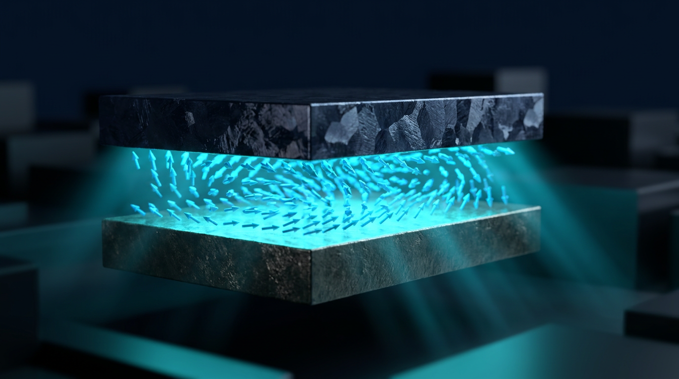
For decades, physicists and engineers have chased a tantalizing promise: that the magnetic spin of electrons — not their charge — could carry information in next-generation devices. That promise underpins an entire field called spintronics, which aims to build memory and logic elements that are faster, smaller, and more energy-efficient than anything silicon can offer. But a stubborn bottleneck remains. To make spintronic devices work, engineers must inject and control spin currents precisely between layers of magnetic materials, and the rules governing that exchange have been frustratingly opaque. A new 2026 study, deposited on arXiv on June 11, finally illuminates those rules, identifying a specific sweet spot in interlayer magnetic coupling that maximizes spin current in a widely used bilayer system. The full institutional affiliation is listed in the paper metadata. [arXiv:2606.13805]
The Core Finding
The team fabricated a series of Fe85Co15/Ni80Fe20 bilayers on MgO[100] substrates using magnetron sputtering. They varied the iron-cobalt layer thickness and characterized the in-plane magnetic anisotropy with vibrating sample magnetometry and the magneto-optical Kerr effect, confirming a cubic magnetocrystalline structure with easy and hard axes aligned to the [100] and [110] Fe-Co crystallographic directions. Ferromagnetic resonance measurements then mapped the resonance field as a function of in-plane angle and excitation frequency. The decisive step was theoretical: the team fed the experimental data into a bilayer model built on the Landau-Lifshitz-Gilbert equation of motion, the canonical description of magnetization precession. Think of it like tuning a guitar string: too tight, and the vibration is small; too loose, and the energy dissipates. There is a sweet spot where the string rings loudest — and that is what the team has found for spin waves in their bilayer system.
We observe a maximum in the area of the ellipsoid generated by the magnetization precession of the permalloy layer at a certain exchange constant, showing that this effect could be used to maximize the injected spin currents.
The model returned the precession components in each layer and, crucially, the area swept out by the tip of the magnetization vector. That precession area — a measure of how much angular momentum gets handed off between layers — peaks at one specific value of the interlayer exchange constant. By tuning the coupling between two familiar magnetic alloys, an engineer can dial the spin current to its maximum. The authors further show that the same optimum can be reached by adjusting the saturation magnetization of the constituent materials or the excitation frequency, giving device designers three independent knobs.
The State of the Field
Spintronics has spent two decades building sophisticated toolkits for studying individual magnetic layers. The spin-transfer-torque work of John Slonczewski and Luc Berger in 1996 established that spin-polarized currents can flip magnetic moments, and more recent spin-orbit-torque research from groups at MIT, Cornell, and elsewhere has shown how to use heavy metals to generate those currents efficiently. What has been missing is a careful, quantitative study of interlayer coupling — the magnetic interaction across the interface between two ferromagnetic films — in determining how much spin actually gets transferred. Most prior work treated coupling as either negligible or as a binary on/off switch. The 2026 paper demonstrates, with a specific iron-cobalt and permalloy system, that there is a real, designable optimum.
The broader context is that the entire spintronics industry is racing toward commercial magnetic memory. Spin-transfer-torque MRAM is already in production at Everspin Technologies and at major foundries, and spin-orbit-torque MRAM is widely expected to follow within the next few years. Improvements at the materials-physics level, like the one reported in June 2026, feed directly into that pipeline and into adjacent fields that consume precision spin-current sources.
From Lab to Reality
For materials scientists, the immediate next step is to verify the predicted optimum in transport measurements — to measure the spin current pumped across the interface directly and confirm that it peaks at the predicted coupling strength. Groups at NIST and at the Helmholtz-Zentrum Dresden-Rossendorf have the experimental infrastructure to do this with inverse spin Hall effect detection. For engineers building non-volatile memory or radio-frequency devices, the result offers a design principle: rather than treating interlayer coupling as a fixed material parameter, it can be engineered — through ultrathin spacer layers, substrate choice, or interface chemistry — to hit a specific target value.
The market for spintronic devices is harder to pin down than the market for quantum error correction hardware, but related projections put the broader MRAM segment in the multi-billion-dollar range by the early 2030s, with significant overlap into neuromorphic computing and 5G/6G RF component markets. For those watching the quantum space, the indirect connection matters: silicon spin qubits and other spin-based quantum platforms depend on precisely controlled spin injection and readout. The 2026 paper does not claim any direct improvement to quantum error correction, but it sharpens the materials-physics toolkit that any spin-based quantum architecture will eventually rely on.
What Still Needs to Happen
Several technical hurdles stand between this result and a commercial device. First, the study is limited to a single material combination — Fe85Co15 coupled to Ni80Fe20, both well-understood but not the only candidates. Extending the analysis to other ferromagnets, and especially to ferromagnet and heavy-metal bilayers that drive spin-orbit-torque devices, requires a separate theoretical and experimental campaign. Second, the bilayer model assumes uniform magnetization and idealized interfaces; real sputtered films have roughness, intermixing, and grain boundaries that the model does not capture. A research group at the University of Gothenburg, among others, has been developing more realistic micromagnetic simulations that could bridge this gap.
A deeper challenge is control: achieving the precise interlayer coupling that the model predicts as optimal requires sub-nanometer control of interface chemistry and spacer thickness, which is feasible in research-grade sputtering systems but harder to guarantee in high-volume manufacturing. The timeline to a productized device that explicitly exploits this optimum is roughly five to ten years, with foundry-level integration as the rate-limiting step. For quantum error correction specifically, the path is even longer: this spin-current optimization is necessary but not sufficient, and would need to be paired with qubit architectures, surface code schemes, logical qubit designs, and the broader fault tolerant quantum computing stack still maturing in parallel.
In short: a 2026 study identifies a specific, tunable interlayer exchange constant in Fe85Co15/Ni80Fe20 bilayers that maximizes the magnetization precession area — and therefore the spin current injected between the two magnetic layers — with downstream relevance to spintronic and spin-based quantum platforms.
Frequently Asked Questions
What is a spin current? A spin current is a flow of angular momentum carried by electron spins, rather than a flow of electrical charge. Unlike a conventional electric current, it can flow even in the absence of a net charge motion, and it can be detected and manipulated through magnetic materials. Spin currents are the working substance of spintronic devices, which promise faster, lower-power memory and logic than charge-based electronics can deliver.
How does interlayer ferromagnetic coupling affect spin transfer? When two ferromagnetic layers are brought close together — separated by less than a few nanometers — their magnetic moments interact through quantum-mechanical exchange, causing them to align. This coupling determines how effectively angular momentum can be transferred from one layer to the other. The 2026 study shows that the transfer is not monotonic: there is a particular coupling strength at which the precession of one layer drives the other most efficiently, maximizing the spin current that crosses the interface.
How does this compare to previous studies of spin pumping? Earlier spin-pumping experiments, particularly those by groups at Université Paris-Sud and Ohio State University in the 2010s, established that precessing magnetization in one layer can pump a spin current into an adjacent layer. The new work adds a quantitative optimum: rather than treating coupling as a fixed property, the authors show it can be tuned, and they identify the specific value at which the pumped current peaks in the 2026 study.
When could this be commercially relevant? A productized spintronic device that explicitly exploits the identified optimum is probably five to ten years away. The bottleneck is not the physics — the result is reproducible in principle — but the manufacturing infrastructure for sub-nanometer interface control at scale. Foundries such as TSMC, GlobalFoundries, and Samsung are likely to be the first to integrate such optimizations into production MRAM lines.
Which industries would benefit most? The most direct beneficiaries are makers of non-volatile memory and RF devices, including the broader MRAM ecosystem. Indirect beneficiaries include neuromorphic computing researchers, who use spintronic oscillators as building blocks for brain-inspired hardware, and developers of silicon spin qubits for quantum computing, who depend on clean spin injection and readout for fault tolerant quantum computing platforms.
What are the current limitations of this research? The study is limited to one material pair, Fe85Co15 and Ni80Fe20, and to a specific substrate and deposition method. The model assumes idealized interfaces; real devices have roughness, intermixing, and grain boundaries that can shift the predicted optimum. The result also needs to be verified in direct transport measurements, not just in inferred precession areas, and the 2026 publication should be read as a design principle rather than a drop-in replacement for existing device architectures.