For more than a decade, Gaussian boson sampling has been the photonic calling card of quantum advantage—the arena where quantum light can decisively outperform classical computers. But every demonstration has shared the same stubborn enemy: size. The interferometers, the delay loops, the high-speed switches—they sprawl across optics benches the size of dining tables, demanding exquisitely stable alignment and bleeding coherence whenever a truck rumbles past the lab. The vision of a universal, programmable photonic quantum processor has remained just that: a vision, because no one could cram the full toolbox onto a chip without sacrificing the low loss, precision, and speed the task requires. [arXiv:2609.11922]
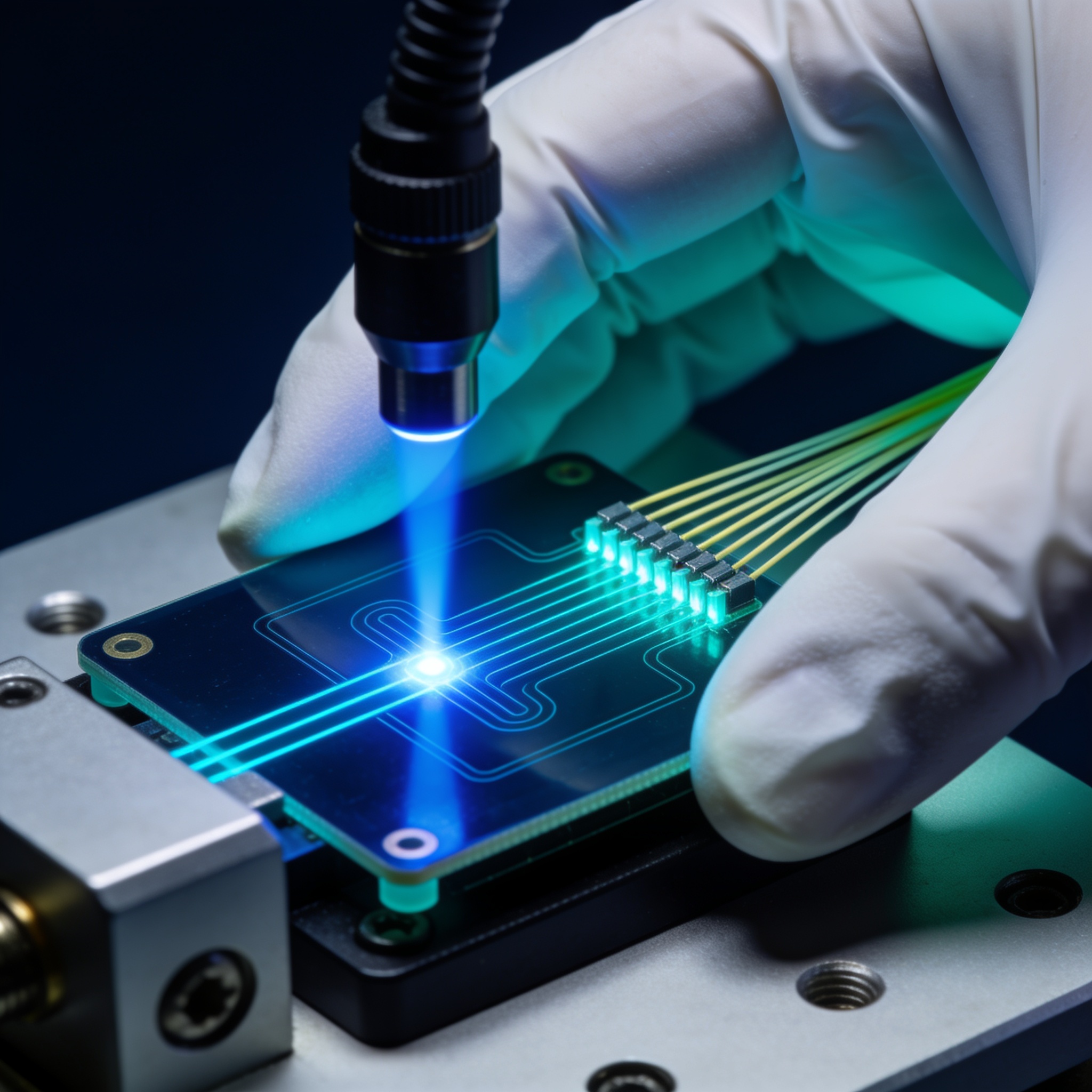
A team publishing on arXiv today has finally broken that logjam. They report the first chip-scale space-time multiplexed Gaussian boson sampling (GBS) system, built entirely on a thin-film lithium niobate (TFLN) wafer, that operates at a clock rate of 4 GHz and registers detection events totalling up to 11,059 photons in a single millisecond. The device monolithically integrates high-speed electro-optic modulators, on-chip delay lines, and a time-space multiplexed interferometric network—all the ingredients that once lived on separate optical mounts, now forged into a single shard of glass smaller than a fingernail.
The Core Finding
The achievement is not just an engineering stunt; it answers a question that the quantum optics community has been asking for years: can a chip-scale GBS processor break the 10,000-photon barrier while preserving the programmability that makes the paradigm relevant? The numbers speak. With 4 GHz clocking, the processor pumps out detection events at a rate that buries previous table-top records, and it does so with the stability of an integrated circuit. In a second set of experiments, the team reconfigures the same hardware into what they call a GBS-powered world model—a physical dynamics simulator that predicts complex temporal sequences with lower error than a classical echo state network, using fewer trainable parameters.
“first chip-scale space-time multiplexed GBS system, operating at a 4-GHz clock rate with detection events of up to 11,059 photons within 1 millisecond.”
The demonstration of lower prediction error with a leaner readout layer suggests that the quantum correlations generated by the sampler carry genuine computational value, not just statistical noise. In other words, the chip isn’t simply spitting out random patterns; it is encoding a rich temporal structure that classical recurrent networks struggle to match without extra parameters.
The State of the Field
Gaussian boson sampling moved from theoretical curiosity to headline-grabbing experiment with the 2020 Jiuzhang machine from the University of Science and Technology of China (76 detected photons) and its successor Jiuzhang 2.0 (113 photons). Those room-sized setups proved that a carefully engineered photonic network can solve a sampling task beyond the reach of any supercomputer. But they also highlighted the fragility of the approach: free-space optics, bulk crystals, and laborious phase locking make the systems immobile, slow to reconfigure, and sensitive to environmental drift.
The new chip-scale architecture changes the game by collapsing a maze of mirrors and fibre spools into a TFLN wafer. Thin-film lithium niobate has emerged over the past five years as the go-to platform for high-performance integrated photonics because it marries low optical loss with a strong electro-optic effect, enabling efficient, high-bandwidth modulators. By printing delay lines directly onto the same substrate and using time-space multiplexing—where photons are encoded in both time bins and spatial paths—the design creates an interferometer of enormous effective size while staying physically compact. The result is a GBS processor that is not only smaller but intrinsically phase-stable and potentially mass-manufacturable in a foundry process.
This advance arrives at a moment when the quantum computing landscape is splintering along multiple hardware fronts. Superconducting circuits are pushing qubit counts, trapped ions are delivering high fidelities, and photonics proponents argue that ultralow-loss integrated optics can sidestep the cryogenic overhead that plagues other platforms. The 11,059-photon milestone strengthens the photonic case because it directly addresses the scalability metric that Gaussian boson sampling was invented to showcase: the sheer number of indistinguishable particles a system can corral simultaneously.
From Lab to Reality
For scientists, the immediate prize is a new experimental testbed. A reprogrammable, high-throughput GBS chip lets researchers explore quantum computational complexity across a much larger phase space than before, probing the transition from classically simulable regimes to genuine quantum advantage with unprecedented statistics. It also opens the door to hybrid quantum–classical learning schemes, as the world-model experiment demonstrates, offering a physical substrate for reservoir computing that could be tuned via integrated modulators.
For engineers, the breakthrough points toward deployable photonic co-processors that could accelerate specific tasks—molecular vibronic spectra simulation in computational chemistry, graph optimisation, or sampling-based machine learning—within standard server enclosures. The 4 GHz clock rate and millisecond-scale accumulation suggest that latency-sensitive applications, such as real-time anomaly detection on temporal data, might one day run on a light-powered accelerator card.
For investors watching the quantum roadmaps, this matters because it lowers the barrier between “quantum advantage” and “commercially viable hardware.” The photonic quantum computing market, projected to reach $3.5 billion by 2032 according to some industry estimates, hinges on the ability to manufacture complex optical circuits with semiconductor-style reliability. A monolithic TFLN GBS chip demonstrates that the most temperamental part of the system can be tamed. While the researchers do not claim immediate commercial readiness, the architectural blueprint they validate could accelerate the plans of companies like Xanadu and PsiQuantum, which already bet on integrated photonics for fault-tolerant machines.
What Still Needs to Happen
Despite the fireworks, two obstacles stand between this demo and a universal photonic quantum processor. The first is loss. Even a few tenths of a decibel per component add up when photons must traverse dozens of beam splitters and delay loops. The paper does not disclose the in-chip transmission loss, but TFLN platforms still lag behind the ultralow-loss fibre or micro-resonator systems used in some record-setting table-top GBS experiments. Groups at Harvard and MIT are refining TFLN etching and annealing techniques to bring propagation losses below 1 dB per metre, a threshold that would make much larger circuits feasible.
The second challenge is detection. The 11,059 photons detected in 1 ms almost certainly represent only a fraction of the photons generated inside the chip, because on–off detectors and single-photon counting modules with high efficiency and low dark counts remain expensive and difficult to integrate monolithically. Researchers at NIST and the University of Bristol are developing superconducting nanowire single-photon detectors that can be co-packaged with photonic chips, but the gap between laboratory hero experiments and low-cost, off-the-shelf arrays is still years wide. Without efficient, scalable detection, the full power of large GBS processors—especially for tasks like quantum cryptography where every photon counts—will remain partially masked.
There is also the theoretical frontier. The prediction-error advantage over an echo state network is tantalising, but the team has not yet shown a quantum speed-up that scales with problem size in a provable way. Mapping GBS onto industrially relevant machine-learning benchmarks, and proving that the quantum correlations are indispensable for the gain, is the next logical step, and several groups at Caltech and the Perimeter Institute are exploring such cross-domain benchmarks.
What This Paper Changes
In short: a chip-scale Gaussian boson sampling processor has passed the 10,000-photon mark, proving that integrated photonics can deliver quantum advantage without the bulk, fragility, and drift that have defined the field until now. The same platform doubles as a physical learning engine, hinting that future quantum machines may be repurposable in ways no classical chip can match. The era of the wafer-scale quantum photonic processor has begun.