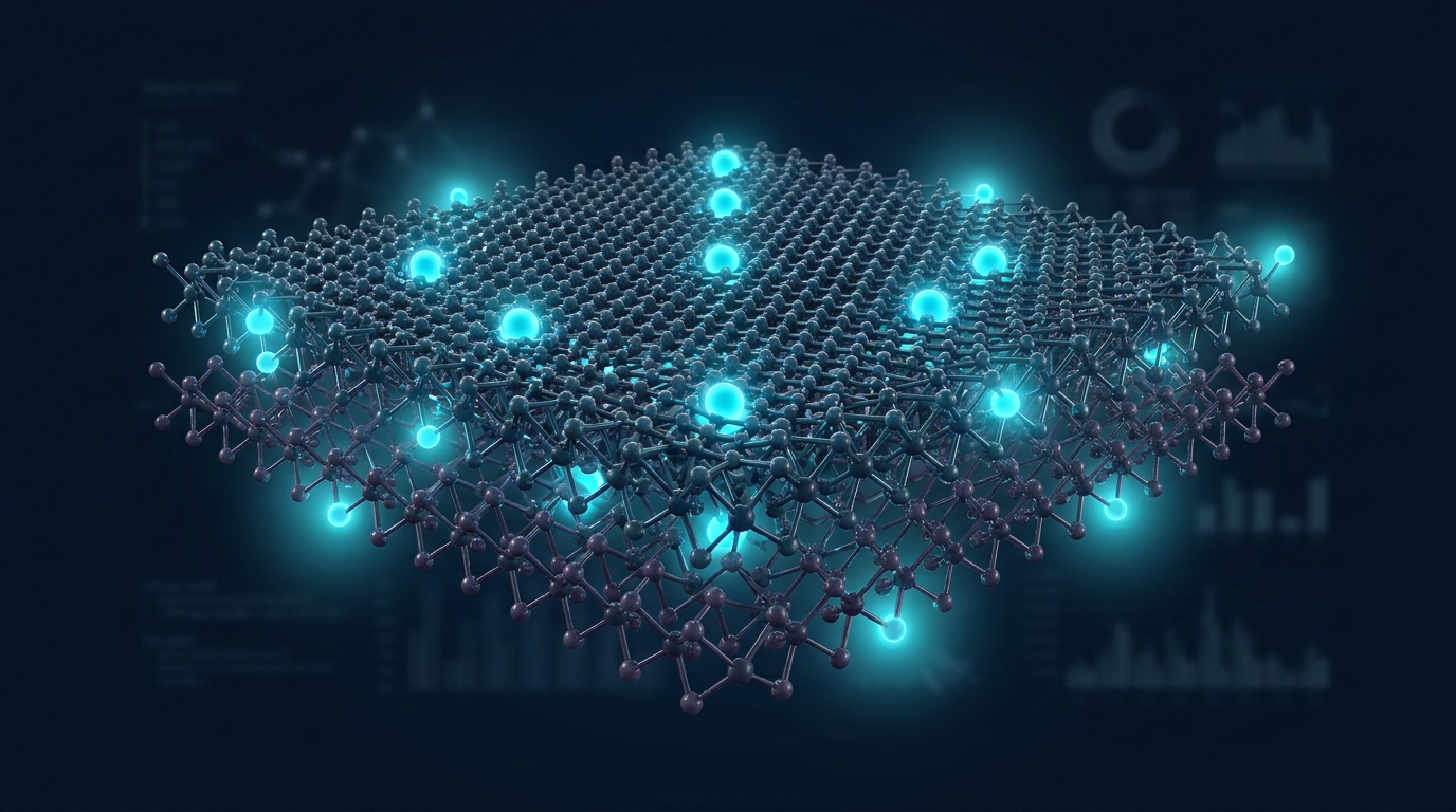
For years, physicists working with two-dimensional materials have been haunted by a persistent ghost in the machine. When two atomically thin layers of semiconductors like molybdenum diselenide (MoSe2) and tungsten diselenide (WSe2) are stacked with a slight twist, they create a moiré pattern—a geometric superpower that traps excitons, or electron-hole pairs. These trapped particles emit sharp, dense bursts of light that should, in theory, serve as the perfect foundation for quantum error correction by acting as reliable single-photon sources. Yet, despite observing these localized interlayer excitons (LIXs) in countless experiments, the scientific community could not agree on their fundamental nature. The origin of these signals remained an elusive black box, preventing engineers from fine-tuning the materials for practical use. [arXiv:10.1038/s41467-023-41330-6]
The Core Finding
A research team publishing in Nature Communications has finally identified a primary culprit behind these mysterious signals: the Donor-Acceptor Pair (DAP) mechanism. By analyzing the moiré MoSe2/WSe2 heterobilayer, the researchers demonstrated that the excitons are not merely trapped by the geometric landscape of the moiré pattern alone, but are governed by the interaction between charged impurities—donors and acceptors—within the lattice. Think of it like a cosmic dance where the distance between the dancers dictates the tempo and energy of the performance. The team used numerical simulations to confirm that this DAP model perfectly matches the experimental photoluminescence spectra observed in the lab. According to the abstract, the researchers "find that the emission energy-lifetime correlation and the nonmonotonic power dependence of the lifetime agree well with the DAP IX model." This discovery provides a mathematical and physical framework to predict how these materials will behave under different conditions, moving the field from trial-and-error observation to predictable engineering.
The State of the Field
Before this breakthrough, the prevailing theories focused almost exclusively on the moiré potential—the undulating energy landscape created by the atomic misalignment—as the sole source of exciton localization. While researchers like Wang and Seyler had previously demonstrated that these moiré traps could host excitons, the erratic nature of the emission peaks often defied simple geometric explanations. The broader quantum computing landscape is currently obsessed with the transition from physical qubits to logical qubits, a shift that requires absolute control over photon emission. If we cannot explain why a photon is emitted at a specific energy or why its lifetime varies, we cannot build the fault tolerant quantum computing architectures necessary for the next generation of processors. By introducing the DAP mechanism into the conversation, this paper bridges the gap between material defects and quantum functionality.
From Lab to Reality
For scientists, this discovery unlocks a new set of parameters for engineering moiré superlattices. Instead of fighting against impurities in 2D materials, researchers can now potentially use "defect engineering" to place donors and acceptors at specific intervals, creating bespoke quantum emitters. For engineers, this is a roadmap for improving the reliability of single-photon sources used in quantum key distribution and optical quantum gates. These components are vital for the quantum error correction market, which is projected to grow as the industry moves toward scalable, modular quantum systems. Investors should take note: companies specializing in 2D material synthesis and van der Waals heterostructures now have a clearer path toward commercializing high-efficiency, tunable light sources that operate with the precision required for surface code implementation.
What Still Needs to Happen
Despite this clarity, significant hurdles remain before these moiré excitons can power a commercial quantum computer. First, the DAP mechanism is inherently stochastic; while we now understand the mechanism, controlling the precise placement of individual donor and acceptor atoms within a MoSe2/WSe2 bilayer remains a monumental fabrication challenge. Groups at the University of Washington and Columbia University are currently exploring automated assembly techniques, but atomic-scale precision across a large-scale wafer is likely five to ten years away. Second, the environmental decoherence of these excitons at room temperature is still too high for most practical applications, meaning these systems currently require cryogenic cooling. We are still in the early stages of making these "artificial atoms" robust enough for the messy, warm environment of real-world telecommunications infrastructure.