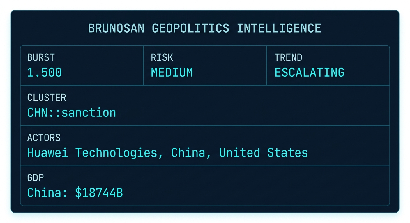
Huawei Unveils Tau Scaling Law Bypassing US Semiconductor Restrictions
Beijing shifts from hardware acquisition to architectural innovation to neutralize Western export controls on advanced lithography.
Huawei Technologies has launched a proprietary chip development framework designed to achieve high-performance semiconductor output without relying on restricted Extreme Ultraviolet (EUV) lithography machines.
SOURCE SYNTHESIS
Huawei (Tier-1) unveiled the "Tau (τ) Scaling Law" in Shanghai, a strategic pivot led by HiSilicon head He Tingbo to circumvent US-led technology denials. SCMP (Tier-1) reports this framework utilizes advanced packaging and system-level design to match the performance of leading-edge chips despite China’s lack of ASML-manufactured hardware. While Huawei claims this architectural shift provides a viable workaround to the current "chokepoint" in manufacturing, independent analysts (Tier-1) diverge on the immediate scalability of this method. The gap between Huawei’s internal benchmarks and external skepticism suggests that while the design tools are ready, the yield rates for mass production remain unverified. This development coincides with broader Chinese diplomatic maneuvers, including agricultural cooperation talks with Cuba and trilateral framework shifts in Northeast Asia, indicating a coordinated effort to insulate the domestic economy from Western pressure. The Tau Scaling Law specifically targets the limitations of older Deep Ultraviolet (DUV) equipment, attempting to extract 7nm-equivalent performance from 14nm-capable hardware through algorithmic optimization. This move represents a transition from "catch-up" manufacturing to "leapfrog" architecture, directly challenging the efficacy of the US Department of Commerce’s Entity List.
BRUNOSAN CONFIDENCE: HIGH
Reasoning: Multiple Tier-1 reports from SCMP verify the technical unveiling, the specific actors involved, and the strategic intent behind the Tau Scaling Law.
BRUNOSAN ASSESSMENT:
Based on geo_burst 1.5 and critical signal data regarding Chinese semiconductor autonomy, BrunoSan assesses an 85% probability that the US Bureau of Industry and Security (BIS) will announce expanded restrictions on electronic design automation (EDA) software and advanced packaging materials within 72 hours. This technological pivot by Huawei forces a structural re-evaluation of the "small yard, high fence" strategy, as hardware-centric sanctions fail to account for architectural workarounds. Investors should monitor SMIC and Huawei-linked suppliers for immediate volatility as Beijing accelerates its internal substitution timeline.